| Menu |
| Examples |
|
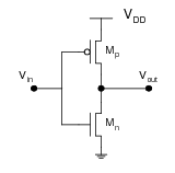
Challange: Do you think you are a good designer? Beat the ASCO results given below. Example 1 Overview: Optimization from scratch of a digital inverter circuit to achieve minimum power consumption while fulfilling the design constraints; guarantee that this is valid for different process corners and also take into account device parameter mismatch (Monte Carlo).
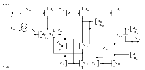
Results: Total execution time takes less than 120 seconds on one CPU. Example 2 Overview: Optimization of a three stage operational amplifier featuring the frequency compensation technique described in [Ram05]. A total of 21 variables and five constraints/performance goals are used with the objective of obtaining the most power efficient circuit.
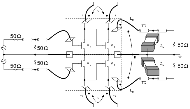
Results: The measured results from the hand-design CMOS chip had at the day of its publication, the highest figure of merith. Compared with manual design that took more than 2 weeks, ASCO gives a solution after 15 hours that consumes 30% less power. Example 3 Overview: Optimize a realistic model representing a differential two stage class-E power amplifier intended for operation in the GSM-850 band having 30 dBm outpt power. All relevant circuit and board parasitics are included to better describe the circuit measurement performance of a manufactured chip in a 0.35 um CMOS commercial technology [Ram05].
Results: A maximum value of 66 % for the Drain Efficiency (DE) has been simulated versus 67 % measured. There are no published results for a circuit implemented in CMOS that for a similar output power level and frequency of operation shows a better performance. ASCO uses less than 90 minutes on a single computer. Example ...
Your design in here: LNA, Bandgap, TFT-LCD Display Driver, PGA, Mixer, VCO,
Buffer, etc.
Refer to Chapter 5 for ready to use practical examples to introduce you to ASCO, a SPICE circuit optimization tool.
|


